Breaking through the boundaries of traditional technology and successfully simplifying the production process, the innovative technology enhances the fineness of the production process, the characteristics of soldering back without residue, the impeccable process results and ultra-high yields, not only a technology, but also a revolutionary breakthrough in the semiconductor advanced packaging process, which is perfectly adapted to the needs of mass production. It is not only technology, but also a revolutionary breakthrough in the advanced semiconductor packaging process, perfectly adapting to mass production requirements.
Precision designed uniform coating technology is applied to various coating applications in electronic and biomedical industries.
We can meet the requirements of customers through various functional products, with good scratch resistance, wear and tear endurance, high levels of transparency, hardness, uniformity, flatness, and anti-smudge ability... or other specifications required by customers.
Using digital printing technology allows targeting only the desired area for tissue staining, saving the cost of expensive Bio-reagents.
It does not only control the usage of reagents more accurately, but also reduce the used amount of wash buffer, and replacement frequency of various reagents, showing its environmental friendly approach.
All this is combined with equipment development and integration capabilities to achieve automation.
We provide solutions for saving time and resources, and achieve higher accuracy in the interpretation of bio-testing results as our customers require.

Using digital printing optimizes the process of setting testing reagents on test strips, by allowing the solution to be placed on the test strip more uniformly and flattened than the original process.
It also provides a method that allows precise integration of multiple detection reagents on the same test strip for multiple functional testing at one time.
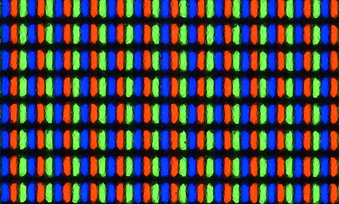
Digital printing technology in combination with newly developed Quantum Dot Ink, enables the development of high-precision equipment for inkjet LED printing and potential mass production applications.
This can simplify the numerous traditional processes for photomask making, and greatly improve material utilization rate.
Reducing material and energy waste in these processes raises Micro LED technology to quickly reach interest as a mass-production solution for the semiconductor industry.
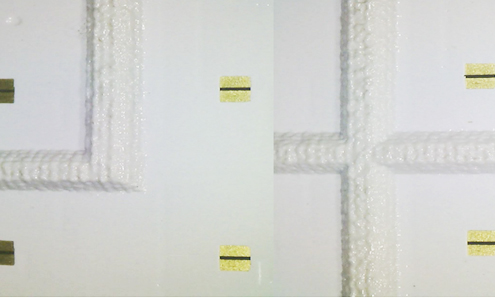
Inkjet technology allows matching special structural designs with special optical function inks to meet the need of specific local dimming applications by customers in the display industry.
This not only improves the contrast efficiency of LED panels, but also enables a more accurate and reliable control of LED backlight modules.

We develop functional inks and printing equipments as complete solution that incorporates into the customer's existing processes, to achieve the uniform light function required by the display industry.
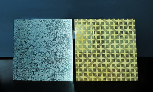
Eliminate the need to invest in photosensitive photoresist materials and expensive related equipment, leaving behind the traditional screen plate opening high-pollution process and reduce printing costs, with excellent corrosion resistance, suitable for all types of nozzles, easy to remove and low viscosity, corrosion-resistant inks for steel panels are virtually VOC-free, a significant reduction of 80% of the wastewater generated, and significantly reduce the amount of cleaning fluid used, to achieve a more economical, reliable and environmentally friendly, bringing the industry a It brings the industry a greener and more efficient future!

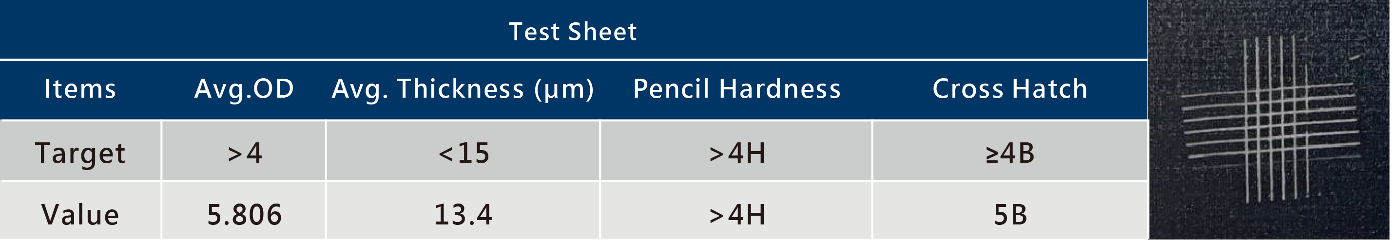
The innovatively developed black border ink for automotive photovoltaic glass effectively replaces the traditional high-pollution plate-making process, providing customized production in small quantities with multiple sizes. It not only has excellent material adhesion (Cross hatch test ≥ 5B), but also has unparalleled optical density (≥ 5 @15um), impeccable display effect, clarity and contrast. The product's high and low temperature resistance and chemical solvent resistance enable it to operate reliably under all kinds of harsh conditions, and Jetbest's black border inks for automotive applications are environmentally friendly, process-simplified, and long-lasting, making them the best choice on the market for cost-effective, reliable performance.